Epitaxial thin films
![]()
Epitaxial
metallic films. Annealing effects
Correlated RHEED and UHV STM studies of epitaxial Ni films grown on MgO
1. (001) Ni growth on (001) MgO.
|
|
|
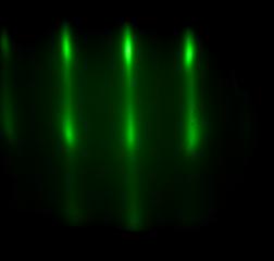
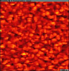
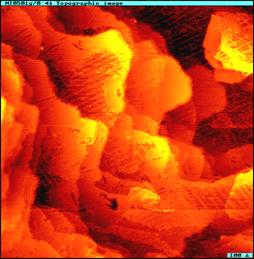
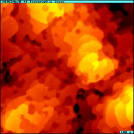
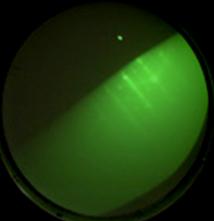
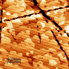
Figure 1. (001) Ni as grown. The RHEED streaks are “spotty” which indicates that the surface is dominated by 3-D mounded features, confirmed by the UHV STM image on the right.
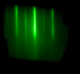
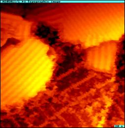
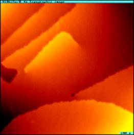
To improve the surface roughness the films
were annealed at 300 C. The RHEED and STM correlated images indicate that the
surface is significantly flatter and now is dominated by 2-D features. The
intermediate streaks observed correspond to 2x1 “missing row” surface
reconstruction due to sub-monolayer surface oxidation.
|
|
|
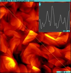
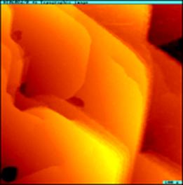
The STM images below show the
(001) Ni surface with higher resolution. We can see details of the 2x1
"missing row" surface reconstruction.
|
|
|
|
Scheme of the 2x1 missing row
reconstruction.
|
|
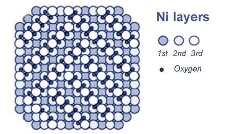
The (2x1) missing row reconstruction has been
observed before, in Mo films grown on MgO. Our RHEED and STM data confirm
“missing row” (2×1) surface reconstruction interpretation in the case of (001)
Ni films grown on MgO.
2. Ni (111) grown on (111) MgO.
|
|
|
Rheed shows thin streaks indicating smooth surface with coarse features. We have extracted from the FWHM an average feature size that is in agreement with the average feature size measured in the STM images.
Subsequent annealing at 300 C leads to
further smoothening and coarsening of the surface features. Top, film surface
after annealed at 150C, and below after annealing at 300C for 1 hour. We notice
in this case that relief of interfacial strain between film and substrate
occurs via dislocations leading to voids in the surface features. Note: The vertical
separation between terraces in the above image corresponds to one atomic
lattice spacing.
|
|
|
We notice evidence of screw dislocation in the figure on the right. This type of dislocation leads to voids and vacancies on the surface as noticed on the right image. The vertical separation between terraces corresponds to one atomic lattice spacing.
We
were also able to identify the presence of a NiO buried layer at the interface
between Ni films and MgO substrates that also appears upon mild in-situ
annealing of the epitaxial Ni films. We have been able to identify a
significant exchange bias effect in epitaxial Ni/NiO films deposited on MgO. (Eur. Phys. J. B.45,
181-184
(2005).
Other epitaxial systems
Epitaxial
graphene
We have recently initiated studies to
elucidate the growth evolution of epitaxial graphene after UHV thermal
decomposition of (0001) 6H-SiC in the temperature range between 1100 C- 1300 C.
We observe that prior graphitization, the SiC surface undergoes several
reconstructions in agreement with previous reports.[i] In
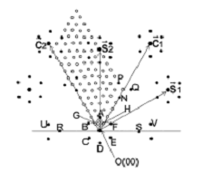
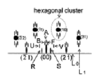
the reciprocal lattice of the 6Ö 3 x 6Ö3 R30o
superstructure, C1, C2 and S1, S2
are the basis vectors of graphite and the 1x1 SiC lattice respectively (Figure
1-c). By comparing the expected RHEED pattern (Figure 1-d) with the actual experimental
one (Figure 1-b) we notice that the R and S streaks are strong enough to be
discerned.
Figure 1. (a)
RHEED pattern of the SiC (0001) surface in the
[10-10] azimuth. (b) Upon annealing at 1100 C for a few minutes the
RHEED pattern exhibits the 6Ö 3 x 6Ö3 R30o surface
reconstruction described in (c) reciprocal lattice of the 6Ö 3 x 6Ö3
R30o SiC superstructure and (d) expected
RHEED pattern along [10-10] azimuth.
|
|
(b) |
(c) |
(d) |
By increasing the
annealing temperature up to 1150 C graphitization of the surface starts to
occur. Nucleation of islands composed of few graphene layers is evidenced after
annealing during 1 minute (Figure 2-center). We observe that further increasing
the annealing time or the annealing temperature leads to significant
graphitization and roughening of the surface. Our ongoing studies will help
understand the evolution of the graphitization process from the early stages of
graphene nucleation.
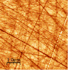
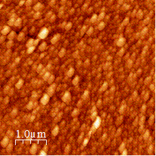
Figure
2. AFM images. (a) Bare SiC. (b) SiC annealed at 1150C for one minute. Small
graphene islands approximately 10 nm in lateral size and a few layers thick are
noticeable on the terraces. (c) After annealing at 1150C during 4 minutes we
observe that the surface exhibits now numerous multilayered graphene islands.
|
|
|
|
Figure
3. Raman scans obtained for HOPG, non-annealed SiC and three samples annealed
at 1150 C, 1250 C and 1350 C for 3 minutes respectively.
|
|
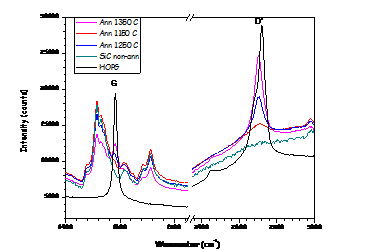
The G band at 1582
cm-1 in the Raman scans of HOPG and the annealed SiC samples is due
to first order (one phonon) Raman scattering process and it is characteristic
of sp2 hybridization. The first order Raman scattering process due
to characteristic zone boundary phonons (at 1325 cm-1) is forbidden
in defect-free structures, but these phonons contribute to the double resonance
Raman process which results in the appearance of the D’ band at ~ 2650 cm-1. This feature is comprised of at least
two-components in graphite but in the case of annealed SiC this band compares
well with that of exfoliated graphene. [ii]
This similarity in the shape of the D’ band strongly supports previous work
pointing towards the quasi-two dimensional Dirac-like character of the electronic
states in graphene-SiC samples.[iii]